Using the serial port - part 2
Introduction
This is the final part to get the serial port of my Alphatronic P2 working again. With the clock generation from the last post Using the serial port - part 1.5 - bitbanging - followup we can now conduct some experiments.
As a preparation I had a close look at the solder straps and added some jumpers so that I can easily switch the operating mode of the serial port.
Hardware side
Luckily I got system documentation which includes the circuit diagram and the information about the possible solder straps. Otherwise it would have been much more puzzling. The serial port allows to run in several modes. And one important mode is, that it can either run using an internal clock or using an external clock. And apparently, the solder straps have been set in such a way, that external clocks are used. These external clocks are fed into the system via the port - it is a 25-pin port, which looks like a standard RS232 port. But it has some proprietary pin assignment to account for the clock lines. Interestingly, the transmit clock and receive clock can be set independently.
Here is the pin assignment of the USART port:
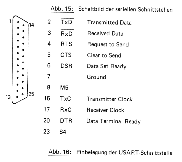
This is taken from “Systemhandbuch Alphatronic”, page 4.4.1/2.
You can see, that there are the standard signals like TxD, RxD and the hardware flow control lines like RTS, CTS, DSR and DTR. But additionally there is TxC (Transmitter Clock) and RxC (Receiver Clock) on pins 15 and 17, respectively.
On the same page, the circuit diagram is shown. It contains a couple of solder straps (a to j), I’ve marked these in red.
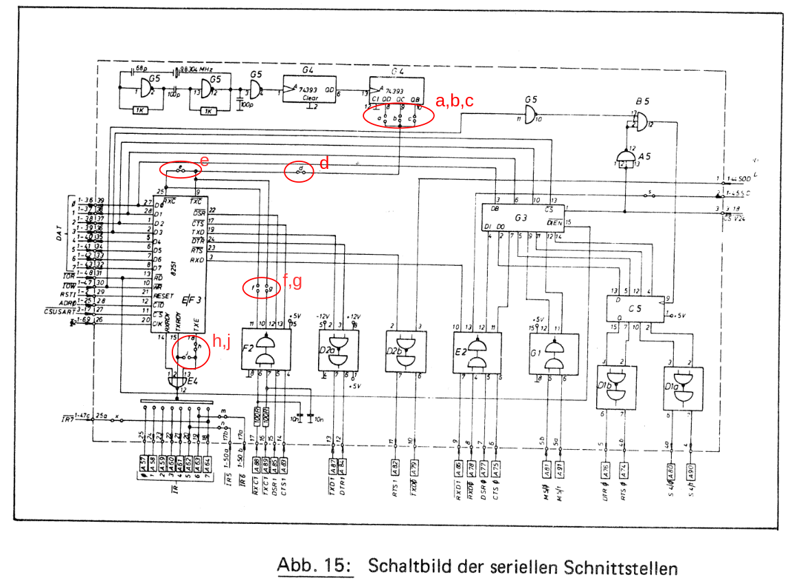
So, there are in 9 solder straps that can change how the serial port operates. There are a couple of more in the diagram, but these are unrelated to our task (m, n, x, s).
On the upper part, you can see the internal clock generation, based on a 9.8304 MHz quartz. There are a couple of dividers following, e.g. G4 (74393) is a dual 4-bit binary counter and the first stage is connected to QD, that means, we divide the clock here by 16. Now we have 9.8304/16 = 614.4 kHz. These can now be further divides, depending on which of the solder straps a, b, or c are closed: if a is closed, we get a internal clock with 614.4/16 = 38.4 kHz; with b closed, we get 614.4/8 = 76.8 kHz; with c closed, we get 614.4/4 = 153.6 kHz. This internal clock is further divided by the serial chip 8251A (oversampling) e.g. by 16, which gives the baudrate:
| closed solder strap | internal clock | baudrate with X16 |
|---|---|---|
| a | 38.4 kHz | 2400 |
| b (default) | 76.8 kHz | 4800 |
| c | 153.6 kHz | 9600 |
Interestingly, the numbers for a and c are swapped in the official documentation, but I guess, this is just wrong. In any case, the factory default is, that solder strap b is closed. And as far as I could figure out by tracing the connections and checking connectivity, this is still the case for the board I have. However, the solder straps a,b,c are so small and are not really recognizable…
On to the next strap - d. This is now a very interesting connection. If this strap is closed, this means that this internal clock is actually connected and used - if it is open, then the internal clock is disconnected and not used. And this solder strap is indeed open on my board. Factory default would have been closed. That explains, why the serial port didn’t work without an external clock signal and it couldn’t send out a single byte. The byte was put into the buffer, but was never sent out and then the chip responded further on with transmitter not being ready, as the buffer is still full and wouldn’t empty.
Then there is solder strap e. This connects or disconnects the transmit and receive clock inputs of the 8251A chip. Factory default is again, that e is closed, so that transmit clock and receive clock are the same. The serial connection sends with the same speed as it receives. But for my board, this was actually open. And with that open, the internal clock will never reach the receive clock input. Which means, if d is closed to use the internal clock, but e is open, then you’ll only be able to transmit data, but never receive anything. That’s why the default configuration is that both d and e are closed.
Then we have two more straps: f and g. These connect the external pins RxC and TxC through a level shifter. Remember, that the physical interface is a RS232 compatible design, that means, that the voltages possibly are between -15V and +15V. That’s not suitable for the 5V TTL chips, and the level shifter (in the diagram marked as F2) is actually a 75154 Quad Line Receiver.
There are two more straps, but I actually didn’t check them. I hope, they are in a state, that doesn’t prevent operation: h and j. These control how the interrupt is created - that is the interrupt of ready to transmit the next byte. If h is closed and j is open, then the interrupt is only created when TxRDY and TxE (the transmitter is actually enabled). If h is open and j is closed, then the interrupt is created already when just TxRDY regardless whether we have enabled the transmitter or not. In my test program, I don’t intend to use interrupts. I plan to poll the status of 8251A to figure out, whether it’s good to send the next byte or whether there is a byte to receive. This is the sample program from documentation and this can’t even send and receive at the same time - it can either receive or either send. Very simple.
Time to have a closer look at the board and try to identify the solder straps.
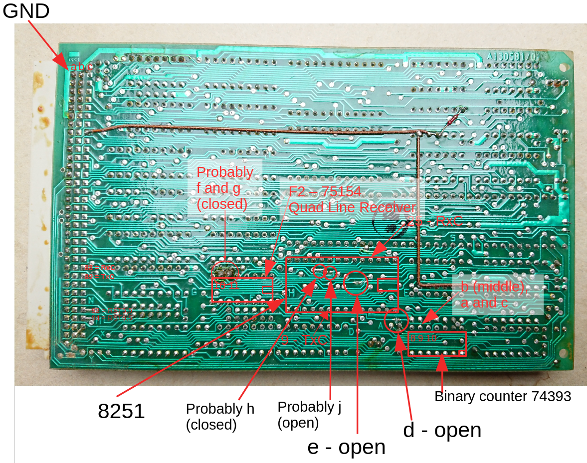
The solder straps d and e are open and you can see some scratches. Highly suspicious. I’ve also marked the location, where I think a,b,c are - directly at the pins of the counter. If you look closely, you can see a trace from the middle pin - which b. But I can’t really see any straps. I suspect, you must scratch open the traces if you want to change the setting here. I anyway want to leave the default, so nothing to do.
Then there are two straps, that look not being tinkered with. These are probably h and j, the ones to control the interrupt. And finally two solder drops, where I suspect the solder straps f and g. These are located near the pins after the line receiver. At least, the two drops are the two pins (10 and 11) of the line receiver, which are connected to TxC and RxC at 8251. That’s why I suspect that the solder straps are below these.
Now the plan is, to bring the board back into factory default - in a reversible way. So I need to solder on some jumpers. I can’t undo what happened to f and g - at least, I won’t try. I just hope, that it doesn’t harm, if the output of the line receiver is connected to the RxC/TxC inputs of the 8251 while the internal clock is also connected. As long as the external clock signals are not driven and the lines are not floating, it might just work. We are anyway not operating at high speeds, so I guess, there is a good chance to be ok.
But I definitely need to close d and e. I want to connect the internal clock - and I want to use the internal clock for both the receiving and transmitting side. I tried to solder some cables directly to the straps, but that’s too small and didn’t retain long. So I decided to solder on the next big pins. That is, I use pin 9 of the binary counter and connect it directly with pin 9 of the 8251 (the TxC pin). For the other connection, there was a pad nearby and a junction at the other side. So, I added two bypasses and that’s how it looks:
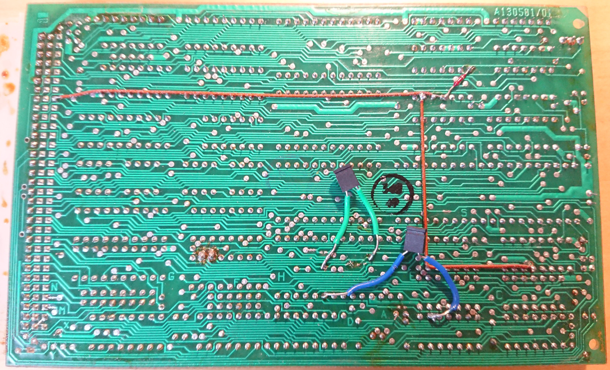
Not super nice, but this should work hopefully.
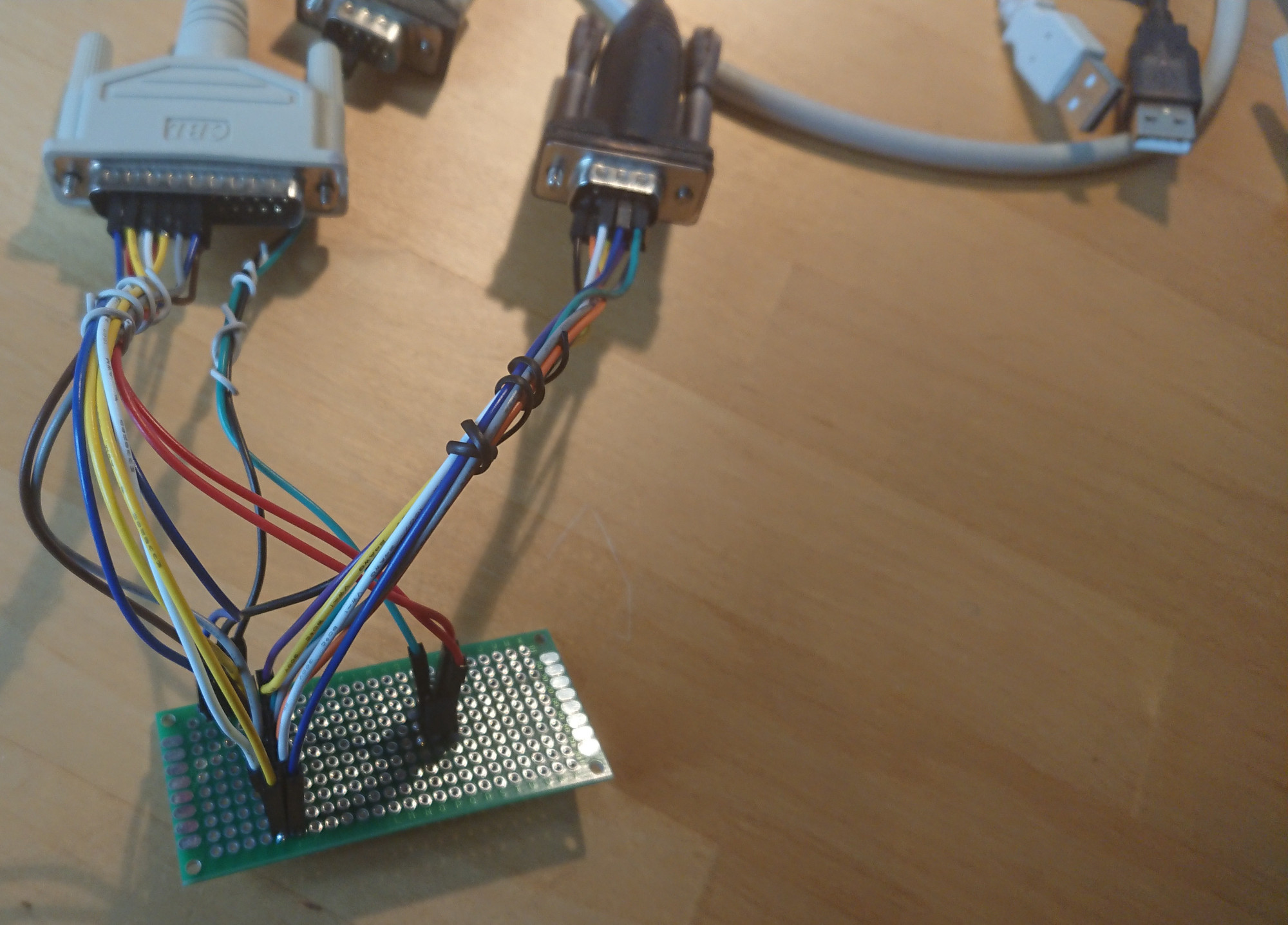
Cabling
As we have seen in the port pin out, there are two extra lines for the external clock. I decided to use a straight 25-pin cable and jumper wires with a small breakout board. The other challenge is, to generate the external clock. In Using the serial port - part 1.5 - bitbanging - followup I described how to generate a clock with a USB serial adapter. To actually try out the serial port of the Alphatronic with external clock, I need 2 USB serial adapters: one for clock generation and one for the “normal” signal lines.
The ground signal is common to the two USB adapters and to the signal ground for the serial port. I only generate one clock signal, which is fed into both TxC/RxC lines. The clock adapter is basically sending, so the TxD line needs to be connected to the clock. And I need to connect the other adapter like using a null modem cable, that means, that TxD and RxD are crossing, as well as RTS/CTS and DTR/DSR.
The whole “product” looks like this - one side is two USB plugs, the other side is a DB25 plug:
Experiment 1
Now we are ready for the first experiment. The jumpers are kept open on the board. That means, we will use an external clock (solder strap d open) and the receive and transmit clock could be different (solder strap e open). Since we feed in the clock on both lines from the special cable, that’s ok. In the end, we will use the same clock from the “usb clock adapter”.
In order to generate the clock, we use the program called JavaSerialClock2 as introduced in the last
post Using the serial port - part 1.5 - bitbanging - followup.
You can also download it from github: adangel/alphatronic-code.
Now we need to start our JavaSerialClock2 program. We need use the correct USB adapter - the one that is supposed
to generate the clock. And we need to set the baudrate variable to e.g. 4800, which gives a clock of 2400 Hz.
~I guess, that actual clock speed is not so relevant, as long as we have a clock.~ Actually, the clock speed matters, because we want to receive with the other USB adapter with a regular terminal program, such as cutecom. Therefore the baudrates must match.
Then we can start the BASIC program to send or receive some data. For the BASIC program, refer to Using the serial port - part 1. On the modern notebook, I used cutecom to drive the second USB adapter.
At first, receiving and sending kind of worked, but the characters were not correct. Sometimes garbage.
The problem was, that 8251A was initialized with the wrong configuration. Somehow I used &H47 in line 540.
And this means actually “1 stop bit, async 64X, 6-bit word”. So, that explains the garbage. I don’t remember,
which experiment this was, but it’s just wrong.
So, when setting the mode byte to &H4D and the baudrate in JavaSerialClock2 to 9600, like so
550 OUT 5,&H4D 'ASYNC, 8 BIT, NO PARITY, 1 STOP, 1X
// Java: int baudrate = 4800 * 2;
it started to work! We generate a clock with 4800 Hz and instructed the 8251 to use asynchronous mode with factor 1 and 8 Bit words and 1 stop bit - or in short: 8n1@4800.
With this setup, it worked to receive and transmit.
In order to make the receiving side more stable, usually 16x oversampling is used. That means, we need to generate a clock at 4800*16=76.8 kHz, like so:
550 OUT 5,&H4E 'ASYNC, 8 BIT, NO PARITY, 1 STOP, 4800 BAUD/16X
// Java: int baudrate = 4800 * 16 * 2;
Note: This is still 8n1@4800.
This configuration worked as well.
However, I noticed that the Alphatronic is very slow on receiving. I needed to use 20ms pause between characters to not miss any. I guess, this is probably due to running the whole thing in BASIC, which does a WHILE loop to poll the received characters.
Experiment 2
The second experiment has the goal to verify, that we can use a normal null modem cable, like the one I created in 2020. Therefore we are going to close the two jumpers, so that solder straps “d” and “e” are closed: We should now use the internal clock and use the clock for both receiving and transmitting.
Note, that the solder straps “f” and “g” are still closed, that means, that a external clock signal could disturb the internal clock, but let’s hope, this doesn’t happen.
We use the same mode setting as in experiment 1, to achieve a 8n1@4800 configuration:
550 OUT 5,&H4E 'ASYNC, 8 BIT, NO PARITY, 1 STOP, 4800 BAUD/16X
On first try, I had partial success: Alphatronic sending worked, but not receiving. Debugging showed, that the BASIC program was waiting on the RxRDY status flag. So, maybe the receiver clock is missing?
And sure, yes, after putting out the board and have a close look again, I saw the problem - bad soldering. The solder strap “e” wasn’t closed anymore, so no clock signal for RxC: “d” connects the internal clock with the TXC input and “e” connects TXC with RXC. That’s why sending worked, but not receiving.
After fixing that (now I used the junctions nearby for soldering), receiving and transmitting worked as it should.
Summary
After long investigations and even hardware modifications, I now have a working serial port again. The serial port works with the regular null modem cable and it uses the internal clock. That means, all the documentation, that assumes internal clock and default solder straps, works.
This serial port could now be used to boostrap CP/M, see the wonderful pages by a former Alphatronic engineer: http://waltroper-aufbruch.de/Archiv/AlphatronicP2.php, http://waltroper-aufbruch.de/Archiv/pdf/PC_V24_AlphatronicP2.pdf and http://waltroper-aufbruch.de/Archiv/pdf/Urleben_P2.pdf.
Comments
No comments yet.Leave a comment
Your email address will not be published. Required fields are marked *. All comments are held for moderation to avoid spam and abuse.